Advantages of observing chips with laser autofocus microscopy systems
Chip observation difficulties:
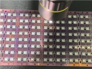
① Tiny size: the size of the chip is usually very small, especially with the continuous progress of semiconductor technology, the circuit structure on the chip is becoming more and more delicate. This makes it difficult for traditional observation equipment to clearly present the details of the chip, and puts forward high requirements for the resolution and magnification of the observation.
② Complex structure: the chip contains a large number of circuit components and complex wiring, with a wide range of hierarchical structures. This makes it difficult to accurately distinguish between different levels and structures when observing, and is easily confused.
③ High requirements for the observation environment: the observation of the chip needs to be carried out under specific environmental conditions, such as dust-free and low vibration. Any small environmental changes may affect the accuracy of the observation results.


Advantages of laser autofocus microscope system for chip observation
1, high-precision autofocus: laser autofocus technology can quickly and accurately lock the focus of the chip, regardless of the surface of the chip high and low or different levels of structure, can always maintain a clear observation picture.
2, high-resolution imaging: the system is equipped with a high-resolution microscope lens, which can magnify and clearly present the tiny structure and details of the chip. Whether it is nanoscale transistors or fine circuit wiring, can be seen at a glance.
3, adapt to complex environments: laser autofocus microscope system on the observation of the environment is relatively low, with a certain degree of anti-interference ability. Even in a slight vibration or a certain amount of dust in the environment, can also ensure the accuracy and stability of observation.
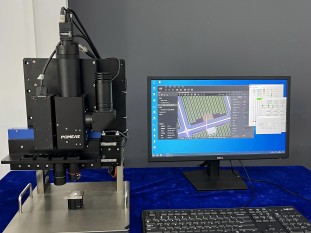
4, efficient and convenient operation: the system has an intelligent operation interface, easy and convenient operation. Engineers can quickly adjust the observation parameters and obtain the required image information. At the same time, the auto-focus function also greatly improves the observation efficiency, saving time and energy.
5, powerful data analysis: laser autofocus microscopy system can not only provide high-quality observation images, but also has a powerful data analysis function. The observed chip image can be measured, labeled, analyzed and other operations, providing powerful data support for chip design, production and quality control.


POMEAS laser autofocus microscope provides an efficient and accurate solution for chip observation with its advantages in focusing accuracy, imaging resolution, environmental adaptability, ease of operation and data analysis, which strongly promotes the development of chip industry.
Product recommendation
TECHNICAL SOLUTION
MORE+You may also be interested in the following information
FREE CONSULTING SERVICE
Let’s help you to find the right solution for your project!


 ASK POMEAS
  PRICE INQUIRY
  REQUEST DEMO/TEST
  FREE TRIAL UNIT
  ACCURATE SELECTION
  ADDRESS
 Tel:+ 86-0769-2266 0867
 Fax:+ 86-0769-2266 0867
 E-mail:marketing@pomeas.com
