1. High precision defect detection:
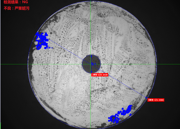
The production of semiconductor chips requires a high degree of precision, and surface defects such as scratches, chipping, and foreign objects can seriously affect the electrical characteristics of the chip and the performance of the final product.FA lenses are able to clearly capture these tiny defects through their high resolution and high contrast, helping inspectors to detect and correct problems in a timely manner. The high resolution ensures that even the tiniest defects can be accurately detected, while the high contrast makes the distinction between defects and their surroundings more obvious, improving the accuracy of the inspection.

2. Automated inspection and identification:
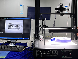
In semiconductor production lines, FA lenses are often combined with advanced image processing software to realize automated defect recognition, size and shape measurement. This automated inspection not only greatly improves the inspection efficiency, but also reduces the interference of human factors and improves the reliability and consistency of the inspection. Through the combination of solution hardware and optimization of software algorithms, FA lenses are able to maintain stable image quality under different lighting conditions, ensuring the accuracy of inspection results.
3. Adaptable to a variety of light sources and environments:
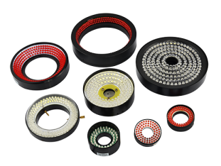
Semiconductor production environments are complex and varied, and the requirements for light sources are also different.FA lenses are characterized by a wide spectral response, which can adapt to a variety of light source conditions, ensuring that high quality image output can be maintained in different environments. This adaptability allows FA lenses to have a wide range of applications in the semiconductor industry and to meet the needs of different production processes.

4. Durability and stability:
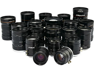
Semiconductor production lines usually require equipment with a high degree of durability and stability in order to cope with the demands of long hours and high-intensity production.FA lenses, as industrial-grade lenses, have been designed with these factors in mind, and are able to maintain a stable performance output in harsh industrial environments. This durability and stability ensures that FA lenses can be used reliably for long periods of time in the semiconductor industry.

5. Improve production efficiency and yield:
By applying FA lenses for automated inspection and identification, the semiconductor industry can significantly improve production efficiency and product yield. Automated inspection reduces manual intervention and speeds up inspection; while high-precision inspection ensures the stability of product quality. These advantages enable the semiconductor industry to better respond to changes in market demand and improve competitiveness.
Product recommendation
TECHNICAL SOLUTION
MORE+You may also be interested in the following information
FREE CONSULTING SERVICE
Let’s help you to find the right solution for your project!

 ASK POMEAS
  PRICE INQUIRY
  REQUEST DEMO/TEST
  FREE TRIAL UNIT
  ACCURATE SELECTION
  ADDRESS
 Tel:+ 86-0769-2266 0867
 Fax:+ 86-0769-2266 0867
 E-mail:marketing@pomeas.com
