


With the rapid development of technology, semiconductor chips are becoming increasingly prominent in industrial applications. From smartphones to data centers, from medical devices to aerospace, semiconductor chips are ubiquitous and support the digitalization process of modern society. However, the problem of surface defects during the chip manufacturing process has been a key factor limiting its performance and reliability. Therefore, efficient and accurate detection of surface defects on semiconductor chips is particularly important.

Measurement Needs:
During the production of semiconductor chips, the presence of surface defects may lead to degradation of chip performance, increase in power consumption or even failure. These defects may include scratches, cracks, contamination spots, bumps, and many other types. In order to ensure the quality and reliability of the chip, it is necessary to perform a comprehensive surface defect inspection.
Solution:
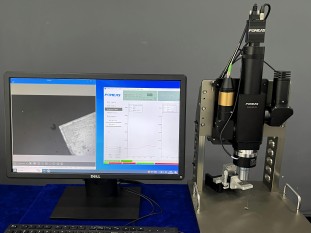
In order to meet the needs of semiconductor chip surface defects inspection, POMEAS launched an advanced semiconductor chip surface defects inspection equipment. The device integrates a high-definition industrial camera, a ten-million-pixel industrial lens and a machine vision light source to realize high-precision and high-speed inspection of the chip surface.
1. High-definition industrial camera: Adopting a high-resolution industrial camera, it is able to capture the minute details of the chip surface to ensure the accurate identification of defects.
2. Multi-Megapixel Industrial Lens: Equipped with multi-megapixel level industrial lens, it provides a wide field of view and clear images, making the inspection process more comprehensive and precise.
3. Machine vision light source: professional machine vision light source is used to provide stable and uniform light conditions for the inspection process, which effectively improves the accuracy and reliability of the inspection.
Program Advantage:
1、High-precision inspection: Through the combination of high-definition industrial camera and ten-million-pixel industrial lens, it is able to realize the precise identification of defects on the chip surface and ensure the accuracy of the inspection results.
2、High-speed inspection: The equipment adopts advanced image processing algorithms and high-speed data transmission technology, which realizes rapid inspection of the chip surface and improves production efficiency.
3、Easy to operate: The equipment is equipped with user-friendly operation interface and intelligent inspection software, which makes it easy for operators to get started and reduces the requirement for professional skills.
4、Expandability: the equipment supports a variety of different types of semiconductor chip inspection, and can be customized and expanded according to customer needs, to meet the inspection needs of different scenarios.
Product recommendation
TECHNICAL SOLUTION
MORE+You may also be interested in the following information
FREE CONSULTING SERVICE
Let’s help you to find the right solution for your project!

 ASK POMEAS
  PRICE INQUIRY
  REQUEST DEMO/TEST
  FREE TRIAL UNIT
  ACCURATE SELECTION
 - APPICATION CASE
- RESOURCE CENTER
- DOWNLOAD CENTER
SOLUTIONS SUPPORT
- ZOOM LENS SELECTION TOOL
- TELECENTRIC LENS SELECTION TOOL
- FA LENS SELECTION TOOL
- ZOOM RATIO TABLE
- CERTIFIED MODEL
SELECTION TOOL
- WHY POMEAS
- FAQ
- PRIVACY POLICY
- TERMS OF USE
- DELIVERY & RETURN POLICY
CUSTOMER CARE
 ADDRESS
Add.:No.68, Chongwei Road, Baizhoubian, East district, Dongguan, China, 523000
CONTACT
 Tel:+ 86-0769-2266 0867
 Fax:+ 86-0769-2266 0867
 E-mail:marketing@pomeas.com

Wechat QR code
Software Copyright :2021SR0176001 抄袭必究, 技术支持:誉新源科技