Silicon wafers are a key part of semiconductor integrated circuits. The production and manufacturing of silicon wafers include multiple processes such as cutting and grinding. These processes are cumbersome and complex and may cause defects such as chipping and cracks in the silicon wafers. These defects will directly affect product quality and therefore require strict testing.
Silicon wafers are precision products with very small surface defects that cannot be identified by the human eye. A high-resolution microscopy imaging system is required for image acquisition to complete defect identification.
Detection Solution:
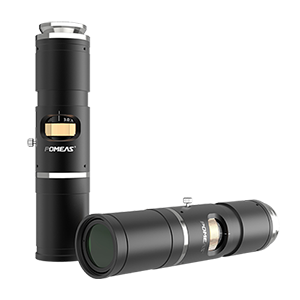
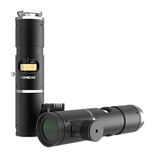
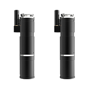
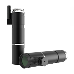
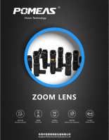
1. The lens uses POMEAS 4K zoom industrial lens;
2. Equipped with 1-inch high-definition CCD camera;
3. Cooperate with POMEAS visual light source and image processing system.
Detection Effect:

The POMEAS 4K zoom industrial lens has the characteristics of large target surface, high resolution, and wide field of view. It can restore the silicon wafer surface image with true high magnification, helping to identify silicon wafer chipping defects faster and easier.
Product recommendation
TECHNICAL SOLUTION
MORE+You may also be interested in the following information
FREE CONSULTING SERVICE
Let’s help you to find the right solution for your project!





 ASK POMEAS
  PRICE INQUIRY
  REQUEST DEMO/TEST
  FREE TRIAL UNIT
  ACCURATE SELECTION
  ADDRESS
 Tel:+ 86-0769-2266 0867
 Fax:+ 86-0769-2266 0867
 E-mail:marketing@pomeas.com
