


Advantages of PCB Ceramic Substrate Inspection with Auto Focus System
In the field of electronic packaging, PCB ceramic substrates are widely used because of their excellent performance. In order to ensure its quality and reliability, high-precision inspection technology is particularly important. As an advanced microscopic observation and inspection technology, laser autofocus microscope system provides strong support for the inspection of PCB ceramic substrates.

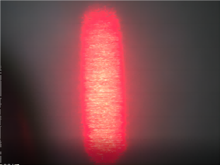
PCB ceramic substrate before focusing

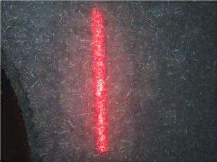
PCB ceramic substrate after focusing
Application of laser autofocus microscope system in PCB ceramic substrate inspection
1, microstructure observation: laser autofocus microscope system can observe the microstructure of PCB ceramic substrate at high magnification, such as circuit wiring, soldering points, components, etc., to help inspectors find potential defects and problems.
2, welding quality inspection: in the manufacturing process of PCB ceramic substrate, welding quality directly affects its overall performance. Laser autofocus microscope system can clearly observe the morphology and structure of the welding point, to determine whether the welding is uniform and solid, so as to ensure the welding quality.
3, cracks and defects detection: ceramic materials are prone to cracks and defects in the manufacturing and use process. Laser autofocus microscope system can accurately detect these subtle cracks and defects, to help manufacturers take timely measures to repair or improve.
Advantages of laser autofocus microscopy systems for PCB ceramic substrate inspection
1, high-resolution imaging: laser autofocus microscope system with high-resolution imaging capabilities, can clearly show the PCB ceramic substrate microstructure, providing inspectors with a wealth of image information.
2, fast autofocus: the system has a fast autofocus function, can automatically adjust the focal length in a short period of time, to obtain a clear image, improve the detection efficiency.
3, non-contact detection: laser autofocus microscope system adopts non-contact detection, will not cause damage to the PCB ceramic substrate, to ensure the integrity and reliability of the sample.
4、Automation and Intelligent: By combining computer vision and image processing technology, the laser autofocus microscope system can realize automation and intelligent inspection process, reduce human error and improve the accuracy and consistency of inspection.

Laser autofocus microscopy system has a wide range of applications and significant advantages in PCB ceramic substrate inspection. With the continuous development of electronic packaging technology, laser autofocus microscopy system will continue to play its important role in PCB ceramic substrate inspection, to improve product quality and reliability to provide strong support.
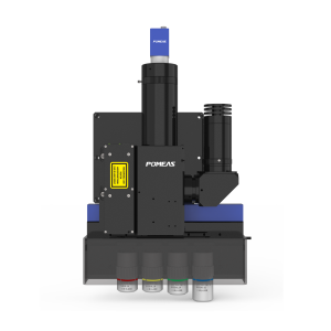
Product recommendation
TECHNICAL SOLUTION
MORE+You may also be interested in the following information
FREE CONSULTING SERVICE
Let’s help you to find the right solution for your project!

 ASK POMEAS
  PRICE INQUIRY
  REQUEST DEMO/TEST
  FREE TRIAL UNIT
  ACCURATE SELECTION
 - APPICATION CASE
- RESOURCE CENTER
- DOWNLOAD CENTER
SOLUTIONS SUPPORT
- ZOOM LENS SELECTION TOOL
- TELECENTRIC LENS SELECTION TOOL
- FA LENS SELECTION TOOL
- ZOOM RATIO TABLE
- CERTIFIED MODEL
SELECTION TOOL
- WHY POMEAS
- FAQ
- PRIVACY POLICY
- TERMS OF USE
- DELIVERY & RETURN POLICY
CUSTOMER CARE
 ADDRESS
Add.:No.68, Yongwei Road, Baizhoubian, Dongcheng District, Dongguan, China,523000
CONTACT
 Tel:+ 86-0769-2266 0867
 Fax:+ 86-0769-2266 0867
 E-mail:marketing@pomeas.com

Wechat QR code
Software Copyright :2021SR0176001 抄袭必究, 技术支持:誉新源科技